|
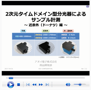
Spectroscopic imaging equipment |
|
 |
|
Spectral imaging device with a new technology which
conventional devices don't have is developed.
Feature or information which cannot be captured by
human eyes or imaging camera can be captured.
|
|
| |
| |
|
Optical related news
|
| |
|
|
|
|
| 2017.05.25 |
|
|
We have won [Spectroscope Innovation Award] for our
lecture at Spectroscope Innovation |
| |
|
|
Research conference of The Spectroscopical Society
of Japan. |
| |
|
|
|
| 2017.05.25 |
|
|
Ichiro Ishimaru, professor at Kagawa University,
has won 21st Century Invention Prize for |
| |
|
|
Encouragement in the commendation category 2 of
Japan Invention Award 2017
of Japan Institute of
Invention and Innovation for [Ultra compact infrared
spectral imaging device(hyperspectral camera).] |
| |
|
|
|
| 2017.05.25 |
|
|
Our spectral imaging device will be exhibited in
'Infrared Array Sensor Forum 2017' |
| |
|
|
(7/21: Osaka Ibaraki campus / Ritsumeikan
University) |
| |
|
|
|
| 2017.05.25 |
|
|
Our spectral imaging device is jointly exhibited
with Vision Sensing at their booth at Image |
| |
|
|
sensing show 2017.(6/7-9 : Pacifico Yokohama) |
|
|
|
|
| 2017.05.13 |
|
|
Lecture, [A flesh development of spectral imaging -
Development and practical usage of Palm-sized |
|
|
|
infrared spectral imaging device (hyperspectral
camera), will be held at Spectroscope Innovation
Research conference of The Spectroscopical Society of
Japan. |
|
|
|
(5/23-25 : Nishi Waseda campus
at Waseda University) |
| |
|
|
|
| 2017.05.08 |
|
|
System that uses our spectral imaging device is
jointly exhibited with 'Kiyohara Optics Inc' |
|
|
|
at their booth at 30th Interphex Japan. |
| |
|
|
(6/28 to 30 Tokyo Big Sight) |
| |
|
|
|
|
2016.12.05 | |
|
We made presentation on our spectral imaging device
at the 14th Annual Meeting of |
| |
|
|
the Japan Association of Medical
Spectroscopy(JTMSTS) |
| |
|
|
|
| 2016.12.02 |
|
|
Mika Ishigaki, assistant processor for Kwansei Gakuin
University, won 2016 NIR Advance Award for |
| |
|
|
[Near-infraered spectroscopy/Imaging Biological
Applications/Industrial Applications,] using our
spectral imaging device in her studies. |
| |
|
|
|
| |
|
|
|
| 2016.12.01 |
|
|
Exhibited at the 5th ANS2016(Asian NIR Symposium
2016). |
| |
|
|
|
| 2016.11.15 |
|
|
Exhibited at the 3rd spectroscopy Fair. |
| |
|
|
|
| 2016.09.15 |
|
|
Development of our spectral imaging device was
acknowledged and |
| |
|
|
[Practical usage of Ultra compact infrared spectral
imaging device(hyperspectral camera)]won Advanced
Analysis Technology Award-JAIMA Instrument Development
Award 2016(The Japan Society for Analytical Chemistry) |
| |
|
|
|
|
| |
|
Applied field of spectral imaging device
|
�
| Band |
1D one shot |
2D time domain |
Application field |
| Visible |
 |
 |
Color evaluation
Bioscience |
Near infrared(1)
Near infrared(2) |
 |
 |
Infrastructure inspection
Food
inspection |
Mid-infrared
Far
infrared |
 |
 |
Resin sorting
Gas analysis |
|
| |
|
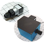
System configuration example of spectroscopic imaging
apparatus
|
| |
 |
|
 |
|
1D one shot |
|
2D time domain |
|
| |
|
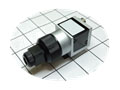
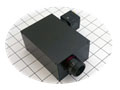
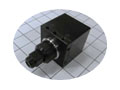
Line up of spectral imaging device
|
|
|
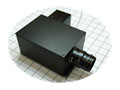
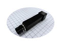
1D one shot type spectral imaging device
|
| |
�
| Model |
Measureable wavelength range |
Size |
Weight |
Resolution |
Interface |
Lens attachment |
| VS00-T030 |
400-1000nm |
Φ18x50 |
0.1kg |
12nm |
USB |
C mount |
| NS00-T011 |
900-1700nm |
Φ15x40 |
0.1kg |
50nm |
LAN |
C mount |
| MS00-T010 |
8-14um |
TBD |
TBD |
TBD |
TBD |
M25 |
|
| |
 |
| |
|
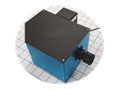
2D time domain type spectral imaging device
|
| |
�
| Model |
Measureable wavelength range |
Size |
Weight |
Resolution |
Interface |
Lens attachment |
| VT01-E011 |
400-1000nm |
120x86x55 |
0.9kg |
10nm |
CameraLink |
C mount |
| NT01-E020 |
900-1700nm |
140x102x60 |
1.2kg |
8nm |
CameraLink |
C mount |
| |
1000-2100nm |
140x102x60 |
1.2kg |
13nm |
CameraLink |
C mount |
| MT01-E020 |
8-14um |
140x12x60 |
1.2kg |
170nm |
CameraLink |
M25 |
|
| |
 |
| |
|
Application examples of spectroscopic imaging equipment
|
| |
|
1.Make concrete life visible. Nondestructive
infrastructure inspection
|
| |
|
|
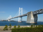 |
Overview |
*Measurement of aging of concrete
*Simplification of inspection of infrastructure such
as brigde or building
*Nondestructive and
no-contact measurement in wide view range
(Case ) ) |
|
| |
|
2.Make food delicioiusness visible. Food component
analysis
|
| |
|
|
 |
Overview |
*Visualize component distribution
such as oil, sugar, moisture, or protein.
*Greasy or delicious part is discriminable in various
food.
*Any sized samples are measurable and kept hygienic
with no-contact method
(Case) |
|
| |
|
3.Make invisible materials visible. Material
identification by infrared light
|
| |
|
|
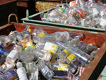 |
Overview |
*Easy discrimination of materials
such as plastic
*Resin color which seems same to human eyes can be
discriminated and identified at one time.
*Suitable
for material separation at recycling site or quality
control
(Case) |
|
| |
|
4.Make invisible change visible. Chemical reaction time
analysis
|
| |
|
|
 |
Overview |
*Visualize invisible chemical
reaction distribution.
*Sensitive measurement contributes to less damage to
samples and to no need for pretreatmemnt such as
staining
*Magnification suitable for application is settable
(Case) |
|
| |
|
Technical data
|
| |
|
|
| |
| |