|
|
|
|
|
|
|
EM Noise Shielding Package |
| |
|
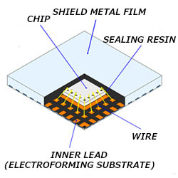
Shield package structure drawing
|
|
| Internal Structure of EM Noise Shielding Package |
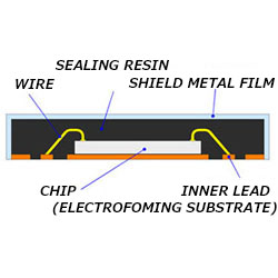
Cross-section of EM Noise Shielding Package |
 |
 |
|
| |
|
|
Features
|
| |
|
Downsizing
|
| ・To allow downsizing compared to conventional metal plate shielding, since there is no need to put mounting pad |
| for metal case connecting. |
| |
|
Low-profile
|
| ・To provide low-profile package by using thinner electroforming substrate (acceptable from Typ 0.30mm). |
| |
|
Noise Reduction
|
| ・To realize higher EMI shield effect by forming shield metal film on the upper surface and four sides of package. |
| |
|
Design Flexibility
|
| ・To allow flexible package design because of independent terminal array pattern forming. |
| |
|
Application
|
| |
・Smartphones, Cellular phones, Tablet
Terminals, Wearable Products
・PC, DSC, Game Consoles,
Household Appliances, Health Care Products
・Satellite
Communication Equipments, Radio Devices(Radar, Aerials,
etc.) |
 |
|
| |
 |
|

Size Data:80KB
|
|
|
|
|
|
|
|
 |
|
|
|
|
|
|
|
|
|
| head office/Takamatsu Plant |
: |
455-1, Kohzai Minamimachi, Takamatsu, Kagawa, 761-8014 Japan |
|
TEL 81-87-882-1131 |
|
FAX 81-87-881-5575 |
|
| Kanonji Plant |
: |
262 Yoshiokacho, Kanonji, KAGAWA, 768-0021, Japan |
|
TEL 81-875-25-5555 |
|
FAX 81-875-23-0020 |
|
| Tokyo Office |
: |
5F,Shinagawa Grand Central Tower, 2-16-4 Konan,Minato-ku,
Tokyo, 108-0075 Japan |
|
TEL 81-3-4221-1112 |
|
FAX 81-3-4221-1113 |
|
| Asahimachi Plant |
: |
3-5-14,Asahimachi,Takamatsu,Kagawa,760-0065 Japan |
|
TEL 81-87-851-2002 |
|
FAX 81-87-823-6234 |
|
|
|
| © 2002 AOI ELECTRONICS CO.,LTD. |
|
|